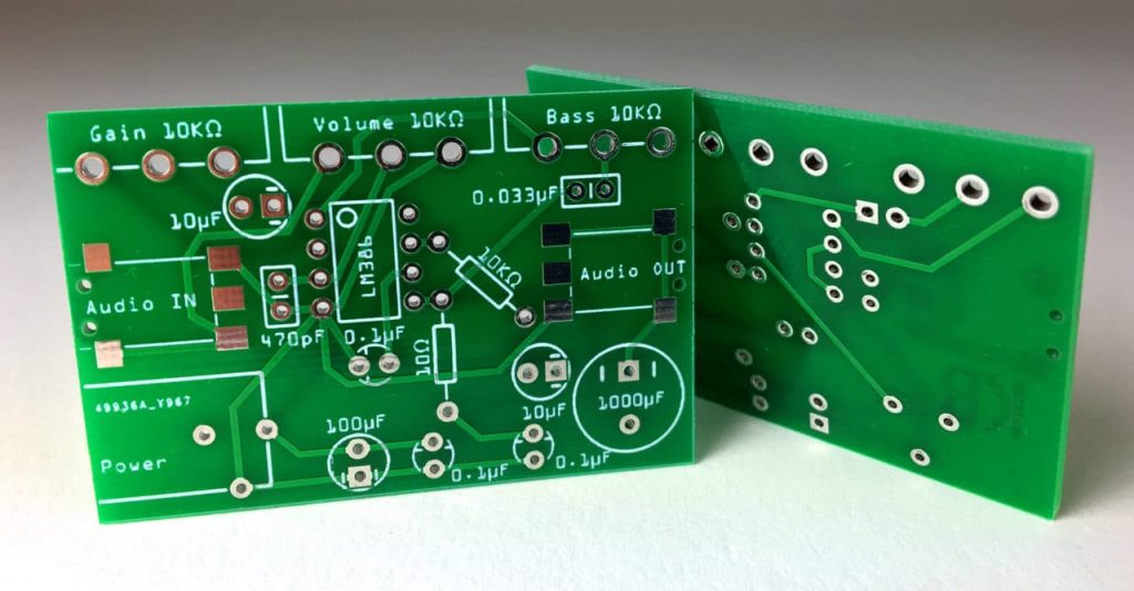
Custom PCB circuit design using CAD is now working in tandem with the generation of the gerber files necessary for the automated production of the board (a gerber file is associated to each layer and not only the metallization ones). It is necessary to decide a priority depending on the complexity of the circuit.
Users can decide whether to develop the PCB automatically or by hand-engraved photoengraving. In the second case, it will be necessary to realize the master of the PCB with enlarged tracks and pitches so that the photo-etching and the pads are easy to use.
The pitches, in particular, must be large enough with respect to the diameter of the holes in order not to be completely removed during the drilling operation itself. The number of layers needed for routing (with the same area) is all the more reduced the less complex the circuit is and the more untangled it is; it is normally a project data.
Two tracks of a PCB, belonging to the same layer of metallization, must develop without intersecting, otherwise they would be short-circuited: this is the main rule (purpose) to be respected (pursued) during the routing.
The unpacking process is often not at all simple, let alone univocal: the designer performs it according to the circumstances and experience. The same circuit can have many different routing solutions, more or less different, all equally valid, but the guidelines to be followed operationally remain the same.
The designer performs the routing using appropriate CADs which use the autorouting function or that of manual routing. Many designers prefer a mixed solution: in a first phase they operate manually on the critical tracks, therefore they complete the routing automatically.
Tools
CAD integrates tools, known as DRC-Design Rule check, that allow to automatically verify the respect of the rules of technology and design (absence of overlaps, width of the posts, minimum distance between tracks, between tracks and pads, etc.).
Before preceding the routing of a PCB it is necessary to establish the boundary: inside the devices and the tracks will be contained. It is also advisable to fix the holes for anchoring the PCB (hole) and to report the dimensions of the PCB and those that identify the position of the connectors or critical components.
To perform the routing in an organic way it is advisable to subdivide the problem into two successive phases: the global routing one and the detailed routing one. Performing global routing means: Define the optimal positioning of the components on the PCB.
Identify (approximately) the paths that the tracks or groups of tracks must follow when connecting the components. Some CADs integrate the automatic placement of the components (automatic placement).
However, the master (PCB designer) generally resorts to manual placement, except for special situations such as that in which there is a base cell that is repeated a high number of times. The preceding points 1 and 2 are strongly interdependent with each other and the trained eye of the designer is fundamental to take them into account appropriately.
An adequate global routing analysis allows to divide the card into a limited number of zones: within each one, a finer routing or detailed routing will be performed.
Routing phase
The global routing phase is delicate as it implies a sufficiently correct assessment or forecast of the density of tracks and obstacles in the different zones (on pain of greater difficulty in the execution of the subsequent detailed routing).
It is necessary to avoid gross errors: if for example there are two devices directly connected to each other, it is useless to arrange them in such a way as to have a third device interposed; moreover, often, exchanging the positions of two connectors (generally located along the edge of the board) can simplify the routing as part of custom PCB design.

